| Sign In | Join Free | My insurersguide.com |
|
| Sign In | Join Free | My insurersguide.com |
|
| Categories | High Density PCB |
|---|---|
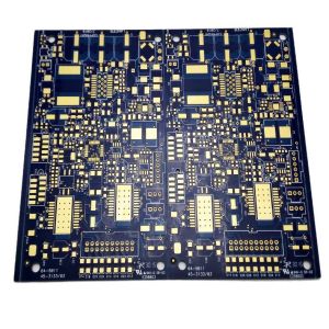
| Brand Name: | High Density PCB |
| Place Of Origin: | China |
| Model Number: | Varies by goods condition |
| Certification: | ROHS, CE |
| MOQ: | Sample,1 pc(5 square meters) |
| Price: | NA |
| Payment Terms: | T/T,Western Union |
| Supply Ability: | 3000㎡ |
| Delivery Time: | 7-10 work days |
| Min. Hole Size: | 0.1mm |
| Pcba Standard: | IPC-A-610E |
| Min. Order Quantity: | 1piece |
| Material: | FR4 |
| Layer: | 1-30 |
| Board Size: | 600X100mm |
| Board Thickness: | 1.2mm |
| Impedance Control: | ±10% |
| Company Info. |
| Dongguan Xingqiang Circuit Board Technology Co., Ltd. |
| Verified Supplier |
| View Contact Details |
| Product List |
| Type | Structure | Typical Applications |
|---|---|---|
| 1-N-1 | 1 HDI layer sequence | Wearables, Basic IoT |
| 2-N-2 | 2 HDI layers per side | Smartphones, Tablets |
| Any-layer | Micro-vias on all layers | High-end CPUs, GPUs, 5G Modules |
| ELIC | Every Layer Interconnect | Aerospace, Medical Implants |
1. Consumer Electronics: Smartphones, tablets, laptops, TWS earbuds, smartwatches, AR/VR headsets, drones.
2. Automotive Electronics: ADAS, battery management systems (BMS), in-vehicle infotainment, central control screens.
3. Medical Devices : Pacemakers, hearing aids, handheld ultrasound devices, endoscopes.
4. Telecom & High-Performance Computing: 5G base stations, high-speed routers, data center servers, AI accelerators.
5. Aerospace & Military Electronics: Radar systems, avionics, satellite modules, missile guidance equipment.
FAQ:
Q: What is the brand name of this PCB product?
A: The brand name of this PCB product is High Density PCB.
Q: Where is this PCB product manufactured?
A: This PCB product is manufactured in China.
Q: What makes the High Density PCB unique?
A: The High Density PCB is known for its compact design and ability to accommodate a high number of components within a small area.
Q: Are the High Density PCBs suitable for high-performance electronic devices?
A: Yes, the High Density PCBs are ideal for high-performance electronic devices due to their excellent signal integrity and reliability.
Q: Can the High Density PCBs be customized to specific requirements?
A: Yes, the High Density PCBs can be customized to meet specific requirements such as size, number of layers, and material composition.

|