Dongguan Xingqiang Circuit Board Technology Co., Ltd.
Dongguan Xingqiang Circuit Board Co., Ltd. was established in 1995 and is a professional circuit
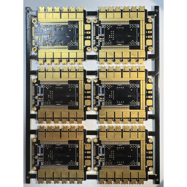
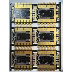
boardfactory that manufactures single-sided and
double-sided PCBs, multi-layer PCBs, and Rigid Flex PCBs.
As a professional supplier of customized boards, we work closely
with our clients, leveraging our strengths in processes and
technologies based on their design files to create
high-performance, high-quality customized boards that support their
product innovation and upgrades.Our company has two production
bases in Dongguan andJiangxi, covering an area of 205000 square
meters with a comprehensive monthly production capacity of 200000
square meters. The company's products are widely used in computer
peripherals, communication, power supply, medical, automotive
electronics, household appliances and other fields.
Our company advocate integrity, win-win and pioneering business
philosophy, and put into practice the work style of "pragmatism,
hard work and responsibility" to create a good corporate
environment. Based on a new management model, advanced technology
and equipment and good product quality, We always adhere to the
corporate spirit of customer first and people-oriented.