| Sign In | Join Free | My insurersguide.com |
|
| Sign In | Join Free | My insurersguide.com |
|
| Categories | MOS Capacitors |
|---|---|
| Delivery Time: | 5-7 working days prototype |
| Breakdown Voltage: | 10-15 MV/cm (oxide breakdown field) |
| Certification: | ISO 9001:2015, RoHS, REACH |
| Payment Terms: | L/C,D/A,D/P,T/T, |
| Oxide Thickness: | Typically 1-10 nm |
| Substrate Material: | Silicon |
| Leakage Current: | Typically in pA to nA range |
| Structure: | Metal-Oxide-Semiconductor |
| Brand Name: | Hoan |
| Model Number: | HACC100S10V101 |
| Capacitance Range: | pF to nF |
| Place of Origin: | Shannxi,China |
| MOQ: | 10 Pieces |
| Temperature Range: | -55°C to 125°C |
| Company Info. |
| HongAn Microwave Co., Ltd. |
| Verified Supplier |
| View Contact Details |
| Product List |
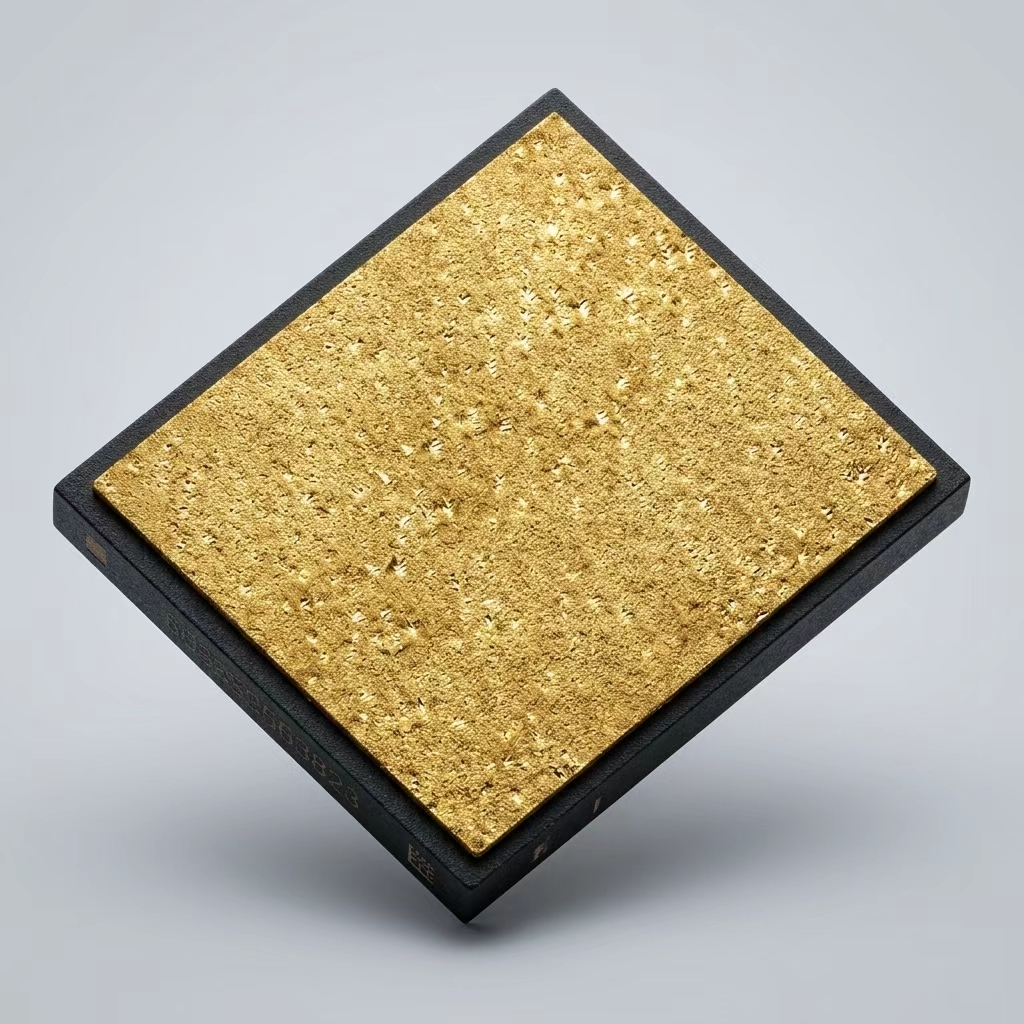
The HACC100S10V101 offers customization of the silicon substrate electrical properties as a design parameter — not a fixed foundry default. N+ or P+ doping profiles are tailored to achieve target resistivity from 0.001 Ohm·cm (heavily doped, low series resistance for high-Q) to 1000 Ohm·cm (lightly doped, minimized junction capacitance for high SRF). The depletion region width under bias is controlled by the doping profile, enabling customer-specified C-V curve shaping: flat capacitance vs. voltage for linear applications, or controlled C-V slope for varactor-like tuning. Resistivity uniformity is ±5% wafer-level and ±2% within-die, verified by PCM (Process Control Monitor) test structures on every wafer. This level of substrate engineering is available because HACC uses a dedicated MOS capacitor foundry process — not a repurposed CMOS logic flow.
Standard MOS capacitors are rectangular dies with a single capacitor plate. The HACC100S10V101 breaks this constraint: custom die aspect ratios, irregular perimeter geometries (L-shape, T-shape, polygonal, annular), multi-cavity array patterns, and rotated or offset pad placement are all supported. This enables capacitor integration into non-standard hybrid circuit footprints — fitting around existing MMICs, waveguide transitions, or thermal management structures — without requiring a separate interposer or PCB. The ability to produce irregular die geometries is enabled by the HACC sawing and singulation process, which supports customer-defined dicing street maps and non-orthogonal die outlines.
A single HACC100S10V101 die can integrate multiple capacitor values in a binary-weighted array: 1:2:4:8 weighting across 4–8 independent capacitor blocks, with capacitance values from 5pF to 1000pF per block. Each block has its own top electrode pad and shares a common backside connection, enabling independent or parallel connection at the hybrid circuit level. Block-to-block isolation exceeds 40dB at 1GHz, and the shared substrate maintains matched temperature coefficient (TCC <30 ppm/°C) across all blocks. This replaces multiple discrete capacitors with a single die, reducing assembly steps, bond wire count, and hybrid circuit footprint — while providing the design flexibility to select any combination of values during wire bonding.
| Parameter | Value |
|---|---|
| Capacitance | 5pF–10,000pF, binary-weighted array blocks |
| Dielectric Type | SiO₂, SiN, Al₂O₃ high-k, 50–5000Å |
| Substrate Resistivity | 0.001–1000 Ω·cm, N+/P+ tailored |
| TCC | <30 ppm/°C (NPO/COG equivalent) |
| Voltage Rating | 6.3V–200V |
| Dielectric Strength | 250% of rated, TDDB >10 years at 125°C |
| ESR | <0.1 Ω at 1 GHz |
| Top Metallization | TiW-Au, Al-metallized, AuSn pre-deposition |
| Bottom Metallization | TiW-Au, TiW-Ni-Au, AuSn, epoxy Au |
| Chip Size | 0.25*0.25mm – 5.0*5.0mm, irregular shapes |
| Operating Temperature | -55°C to +125°C |
| Delivery | Gel-Pak, waffle pack, tape-and-reel, wafer-level |
Contact us with your target capacitance values, substrate resistivity, and die geometry requirements. Custom MOS capacitor prototypes with binary array integration ship in 5–7 business days.
|
 Ultra High SRF 100pF 25V MOS Capacitor Conductive Silicon Substrate Direct Grounding Single Layer RF Chip
Ultra-Low Leakage 150pF 100V MOS Capacitor High Dielectric Breakdown Strength Extreme Thermal Endurance SLC Chip
Custom Multi Capacitor Array 4 Channel 100pF 30V MOS Capacitor 100 Percent Wafer Level Tested SLC Chip
Miniaturized High-Density 220pF 30V MOS Capacitor Exceptional High-Frequency Stability Wafer-Level Custom SLC Chip
High-K Dielectric 330pF 25V MOS Capacitor Ultra-Low Phase Noise Wire Bondable Single Layer Chip for VCO PLL Circuits
Custom High Breakdown Voltage Low Leakage 1000 pF MOS Capacitor Ultra Stable TCC Wire Bondable Chip for RF Bypass
Ultra Small 0.40mm Bare Die Radiation Hardened 47pF 50V MOS Capacitor Zero Piezoelectric Noise Single Layer Chip
Custom High Q Ultra-Low ESL 470 pF MOS Capacitor Wire Bondable Single Layer Chip for RF Microwave Circuits
Zero Dielectric Memory 1000pF 80V MOS Capacitor Ultra-Linear CV Characteristics Paraelectric SiO2 Single Layer RF Chip
Low Dissipation Factor 50pF 50V MOS Capacitor Custom Metal Metallization SLC Chip for RF Power Packaging
Ultra High SRF 100pF 25V MOS Capacitor Conductive Silicon Substrate Direct Grounding Single Layer RF Chip
Ultra-Low Leakage 150pF 100V MOS Capacitor High Dielectric Breakdown Strength Extreme Thermal Endurance SLC Chip
Custom Multi Capacitor Array 4 Channel 100pF 30V MOS Capacitor 100 Percent Wafer Level Tested SLC Chip
Miniaturized High-Density 220pF 30V MOS Capacitor Exceptional High-Frequency Stability Wafer-Level Custom SLC Chip
High-K Dielectric 330pF 25V MOS Capacitor Ultra-Low Phase Noise Wire Bondable Single Layer Chip for VCO PLL Circuits
Custom High Breakdown Voltage Low Leakage 1000 pF MOS Capacitor Ultra Stable TCC Wire Bondable Chip for RF Bypass
Ultra Small 0.40mm Bare Die Radiation Hardened 47pF 50V MOS Capacitor Zero Piezoelectric Noise Single Layer Chip
Custom High Q Ultra-Low ESL 470 pF MOS Capacitor Wire Bondable Single Layer Chip for RF Microwave Circuits
Zero Dielectric Memory 1000pF 80V MOS Capacitor Ultra-Linear CV Characteristics Paraelectric SiO2 Single Layer RF Chip
Low Dissipation Factor 50pF 50V MOS Capacitor Custom Metal Metallization SLC Chip for RF Power Packaging

