| Sign In | Join Free | My insurersguide.com |
|
| Sign In | Join Free | My insurersguide.com |
|
| Categories | Sapphire Wafer |
|---|---|
| Brand Name: | zmsh |
| Place of Origin: | China |
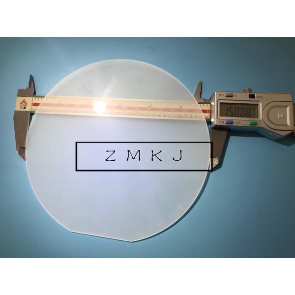
| Model Number: | Sapphire Wafer 6'' Dia 150mm±0.1mm Thickness 1000um |
| Certification: | rohs |
| MOQ: | 20 |
| Price: | 5 |
| Payment Terms: | T/T, Western Union |
| Supply Ability: | 10000per month |
| Delivery Time: | 3-4 week |
| Packaging Details: | Carton box |
| Material: | >99.99% Sapphire |
| Orientation: | C-Plane(0001) |
| Diamater: | 150±0.2mm |
| Thickness: | 1000±10um |
| Warp: | ≤20um |
| BOW: | -15um≤BOW≤0 |
| TTV: | < 10 um |
| Polished: | SSP Or DSP |
| Company Info. |
| SHANGHAI FAMOUS TRADE CO.,LTD |
| Verified Supplier |
| View Contact Details |
| Product List |
Sapphire Wafer 6" Dia 150mm±0.1mm Thickness 1000um C-plane 99.99%pure
Our 6-inch diameter sapphire wafers are precision-engineered single crystal Al₂O₃ substrates designed for demanding semiconductor applications. With strict diameter control at 150.0±0.1mm and standard thickness of 1000±15μm, these C-plane (0001) oriented wafers deliver exceptional performance for:
Specifications
Parameter | Specification |
|---|---|
| Diameter | 150.0 ±0.1 mm |
| Thickness | 1000 ±10 μm |
| Orientation | (0001) ±0.15° |
| TTV | <10 μm |
| Warp | ≤20 μm |
| Bow | -15um≤BOW≤0 |
| Warp | <10 μm |
Applications of Sapphire Wafers
Sapphire Wafers in Optoelectronics
Sapphire Wafers in Power Electronics
Sapphire Wafers in Emerging Technologies

KEY Features of Sapphire Wafer
1. Sapphire Wafers's Superior Thermal Performance
2. Sapphire Wafers's Optical Excellence
3. Sapphire Wafers's Mechanical Robustness
4. Sapphire Wafers's Manufacturing Advantages
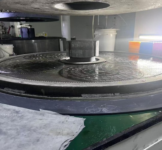
Sapphire Wafer manufacture process
1. Orientation: Accurately locate the sapphire crystal rod position on the slicing machine, so as to facilitate precise slicing processing

2. Slicing: Cut the sapphire crystal rod into thin wafers
3. Grinding: Remove the chip cutting damage layer caused by slicing and improve the flatness of the wafer
4. Chamfering: Trim the wafer edge into a circular arc to improve the mechanical strength of the wafer edge to avoid the defects caused by stress concentration

5. Polishing: Improve the roughness of the wafer to reach the epitaxial wafer's precision

6. Cleaning: Remove the contaminants on the wafer surface (such as dust particles, metals, organic contaminants)
7. Quality inspection: The wafer's quality (flatness, surface dust particles, etc.) shall be inspected with high-precision testing instruments to meet customer requirements

|
